
| Smart Card
Technology: Introduction To Smart Cards
by Dr. David B Everett.
Return to page 1
Physical characteristics of the Contact Card Many observers have commented that the widespread use of Smart Cards is being impeded by the lack of standards. Interoperability is of course the name of the game and is the primary purpose of standards. The problems of interoperability start at the bottom, in other words with the physical dimensions of the card and the location of the contacts. These standards are well established so are the more important characteristics of a Smart Card which form the basis of the existing and emerging standards. As you move higher in the architecture towards the specification of the application then the problems of interoperability are less relevant since it is not generally necessary to have compatibility between the applications themselves. The biggest hole in the current standards work is the lack of agreement in the security domain which one might argue is fundamental to the application platform. The physical characteristics of an IC card are defined in ISO 7816 part 1. This standard applies to the ID - 1 identification card specified in ISO 7810 and includes cards which may have embossing or magnetic stripes. While we are all familiar with the use of imprinters to obtain a printed version of the embossed characters on some paper voucher, their viability on an IC card must be questionable. The IC module in a Smart Card is like any other electronic component and is not normally expected to be hit with a hammer at regular intervals. Even the embossing process itself is mechanically stressful and must raise serious doubts over the appropriate migration strategy. The physical properties of the contact IC card are referenced against earlier card standards and we will look at each of them in turn. ISO 7810 Identification cards - Physical characteristics (1985) This standard specifies the physical characteristics of identification cards including card material, construction, characteristics and nominal dimensions for three sizes of cards (ID -1, ID -2 and ID -3). It is the ID -1 card that forms the basis of ISO 7816 -1. The principal parameters of ISO 7810 are the dimensions of the ID -1 card which are defined to be, 85.6mm x 53.98mm x 0.76mm ISO 7811 Identification cards - recording techniques (1985) This standard is in five parts and covers the specification of the magnetic stripe and the card embossing. Part 1 Embossing This part specifies the requirements for embossed characters on identification cards for the transfer of data by imprinters or by visual or machine reading. Part 2 Magnetic stripe This part specifies characteristics for a magnetic stripe, the encoding technique and coded character sets which are intended for machine reading. Part 3 Location of embossed characters on ID -1 cards. As the title implies, this part of the standard specifies the location of embossed characters on an ID -1 card for which two areas are assigned. Area 1 is for the number identifying both the card issuer and the card holder. Area 2 is provided for the cardholder identification data such as his name and address. Part 4 Location of magnetic read only tracks - tracks 1 and 2 This standard specifies the location of the magnetic material, the location of the encoded data tracks and the beginning and end of the encoding. Part 5 Location of read - write magnetic track - track 3 This standard has the same scope as part 4 except that it defines the read - write track 3. ISO 7812 Identification cards numbering system and registration procedure for issuer identifers (1987) This standard relates to the card identification number or PAN (Primary Account Number) which consists of three parts, the issuer identifer number (IIN), the individual account identifier and the check digit. ISO 7813 Identification cards - Financial transaction cards (1987) This standard defines the requirements for cards to be used in financial transactions. It specifies the physical characteristics, layout, recording techniques, numbering system and registration procedures. It is defined by reference to ISO 7810, ISO 7811 and ISO 7812. In particular the standard defines more precisely the physical dimensions of the card as follows:
This device often consists of a movable carriage that positions the card under the connector head while applying the necessary wiping and pressure action.Variation in thickness or even slight warping of the card can cause communications failure. ISO 7816 Design and use of identification cards having integrated circuits with contacts (1987) This standard in its many parts is probably the most important specification for the lower layers of the IC card. The first three parts in particular are well established and allow total physical and electrical interoperability as well as defining the communication protocol between the IC card and the CAD (Card Acceptor Device). Part 1 Physical characteristics The physical dimensions of the IC card are defined as that specified in ISO 7813. It should be noted that the thickness dimension does not include any allowance for embossing. More particularly the slot for a card may include an extra indentation for the embossed area of the card. In effect it acts as a polarisation key and may be used to aid the correct insertion orientation of the card. This is an additional characteristic to the magnetic field sensor which operates off the magnetic stripe and is used to open a mechanical gate on devices such as ATMs where some vandal proofing techniques are required. The Part 1 standard also defines additional characteristics that should be met in the manufacturer of an IC card. These characteristics fall into the following categories:
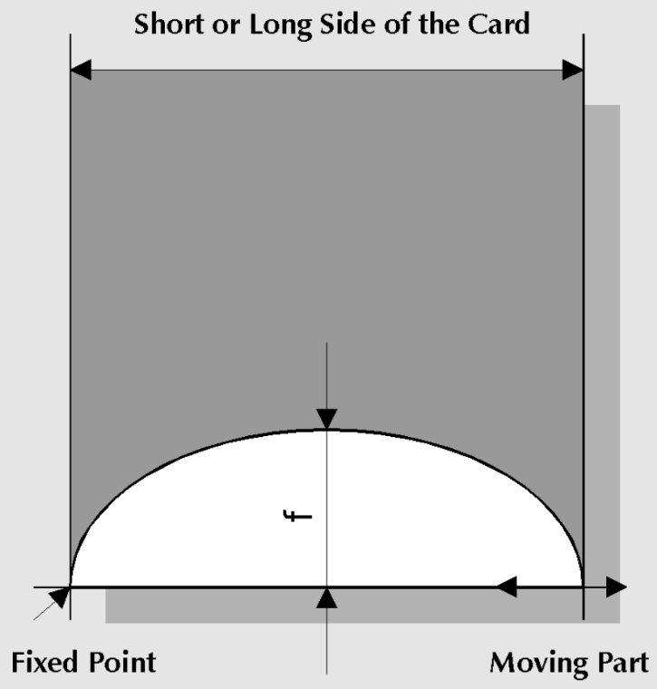
The bending properties are tested by deflecting the card on each axis as shown in figure 6. With a periodicity of 30 bendings per minute the card is deflected to 2cm at its centre from the long axis and 1cm from the short axis. The recommended test requires the card to withstand 250 bendings in each of the four possible orientations (i.e 1,000 bendings in total). The torsion properties of the card are tested by displacing the card + 15o about the long axis at a periodicity of 30 torsions per minute figure 7. The standard requires the card to withstand 1,000 torsions without chip failure or visible cracking of the card. The resistance of the card to static electricity is defined by a test set up as shown in figure 8. The test voltage is defined to be 1.5KVolts. The specification requires this voltage to be discharged across each of the contacts in both normal and reverse polarity. The IC should still be operational at the end of the test. One of the issues surrounding the use of the IC card relates to the temperature range for operational use. ISO 7810 defines that the ID-1 card should be structurally reliable and usable between -35oC and +50oC. The draft CEN standard on requirements for IC cards and terminals for telecommunications use, part 2 - application independent card requirements (EN 726-2) defines more stringent requirements for operational use as -25oC to +65oC with occasional peaks up to +70oC. In addition the draft identifies multi-application cards for portable battery operated equipment to be used between -25oC and +70oC with occasional peaks of up to +85oC. The word occasional is defined to mean not more than four hours each time and not over 100 times during the life of the card. ISO 7816 Part 2 - Contact Locations and Minimum Size This part of the standard has taken a lot of effort in order to reach agreement. Early applications of Smart Cards emanated in France where the Transac magnetic stripes were more central on the card than that eventually defined by ISO 7811. Unfortunately the French chip position overlaps the ISO magnetic stripe definition. As a result it was eventually agreed that after a transitional period (to the end of 1990) the position for the IC connector would be as shown in figure 9. This position is much closer to the longitudinal axis of the card. We might like to conjecture on which is the better position for the chip in terms of mechanical stress but perhaps we should just settle for agreement. Further problems arose in deciding on which face of the card the connector should be located. In order to avoid further delay in publishing the standard, two options were allowed to include both the front and back of the card. This anomaly has been a source of irritation and it is now widely agreed that the IC connector should be on the front of the card. For this purpose the back is defined to be the side with the magnetic stripe. The embossing is defined to be on the front of the card and therefore on the same side as the IC connector. The relative location of these components (when present) is shown in figure 10. Electronic signals and transmission protocols. The electronic properties and transmission characteristics of the IC card are fundamental to interoperability. These specifications are defined by ISO as part three of the 7816 standard. This standard is subject to an amendment for the T=1 transmission protocol and a proposed review for protocol type selection (PTS). The principal subjects to be considered are as follows:
IC Card electrical characteristics We have previously discussed the position and definition of the IC connector and have identified eight contacts of which six are currently defined,
The power supply to the IC is defined to be between 4.75 volts and 5.25 volts with a maximum current consumption of 200mA. Both of these parameters have problems. Newer chip fabrication technologies are moving sub micron, 0.8um is already commercially available and 0.5um is not that far away. These chips may operate with a supply voltage of 3volts which results in lower current consumption. Most card acceptor devices (CAD) operate at 5volts as specified in the ISO standard. while a 3volt IC may be designed to operate between 3volts and 5volts, running a 5volt IC at 3volts is a non starter. A current consumption of 200mA is far too high for modern electronic equipment particularly when the equipment is portable and driven by a battery power supply. Most IC cards have a power consumption of between 10mA and 20mA (at 3.58MHz). ETSI in the development of its standards has adopted a far more rigorous specification of 20mA maximum for normal use and a 10mA maximum for use in portable equipment. It further defined the concept of sleep mode (not covered by ISO 7816-3) where the IC chip can reside in a latent mode preserving volatile memory contents with a maximum power consumption of 200uA. Clock signal Although the integrated circuit could contain its own clock circuit for driving the internal logic, in practice most IC chips are supplied with an external clock by the interface device. It should be noted that the speed of the serial communications on the I/O line is effectively defined by the frequency of this clock. The ISO standard aligns with the use of two widely used external clock frequencies, 3.579545 MHz and 4.9152 MHz. The former frequency is the more widely used (being based on the NTSC colour sub carrier frequency) and results in a clock divider of 372 in order to produce a 9600 bit per second (not exact but within tolerance) serial communication speed. The latter frequency has a simple divisor of 512 in order to achieve a 9600 bit per second communication speed. The standard defines the situation after reset whilst allowing the frequency to be selectively changed by means of protocol type selection. Programming voltage VPP This signal is designed to provide the high voltage required to enable writing to the non volatile memory. The more popular ICs use EEPROM memory where the high voltage is generated by a charge pump on chip. However the EPROM memory type needs the high voltage (usually 12.5V or 21V) to be externally provided on the IC connector. There have been problems in the past with terminals supplying the wrong programming voltage with somewhat drastic effects. Because of this and the significant advantages of having a rewriteable memory, the EEPROM memory is by far the most popular for IC card applications, hence the role of VPP is rapidly diminishing. The reset signal The reset signal is asserted by the interface device and is used to start up the program contained in the IC ROM. The ISO standard defines three reset modes, internal reset, active low reset and synchronous high active reset. Most microprocessor ICs operate using the active low reset mode where the IC transfers control to the entry address for the program when the reset signal returns to the high voltage level. The synchronous mode of operation is more commonly met with the memory card ICs as used for telephone applications. The sequence of operations for activating and deactivating the IC is defined in order to minimise the likelihood of damage to the IC. In particular the inadvertent corruption of the non-volatile memory (EPROM or EEPROM) must be avoided. The activation sequence for the interface device is defined as follows,
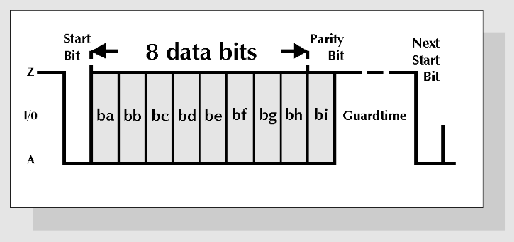
The ISO standard defines a single line for the interchange of data between the IC and the interface device. This means that the line must change direction depending on whether the IC is transmitting or receiving. In practice this cannot be instantaneous and the expression "line turnaround time" is commonly encountered in the modem world. The transmission protocol must take account of this need to turn the line around. Character Transmission The transmission characteristics operated by most microprocessor IC cards are based on an asynchronous half duplex mode of operation. In the T=0 communication protocol, this involves the transmission of bytes whilst the T=1 protocol defines a block mode of operation. As we have already observed the serial communication is operated by the use of a single chip connector, where the direction of data transmission has to change depending on whether the IC card or interface is transmitting data. This is referred to as half duplex communication whereas two I/O signal connectors would be required for full duplex operation where transmission can take place in both directions concurrently. The asynchronous type of transmission is similar to that used by the serial RS232C connector met on the personal computer. Although the PC operates in full duplex mode. The transmission of a single character (defined as 8 bits) requires an overhead of several bits as follows:
The guard time is defined to be equal to two bit periods (although for block mode it can be changed to a 1 bit period). This is similar to having two stop bits on a UART (Universal Asynchronous Receiver Transmitter) as used in the PC. A more common definition of the asynchronous serial transmission at reset would be 9600 bits/second, 8 data bits, even parity, 2 stop bits with half duplex mode of operation. The half duplex refers only to data transmissions in one direction at a time which a PC is perfectly capable of managing with its UART. The RS232C interface however defines two separate wires for data transmission and reception which would need hardware modification in order to interface with the single wire IC card directly. There is a further problem with the asynchronous character transmission that makes life difficult for a PC to act as the interface device. The 7816-3 standard defines an error detection and recovery operation (mandatory for T=0) that cannot be managed by the normal PC UART. When the receiver detects a parity error on reception it takes the I/O line to the space or low state in the middle of the first stop bit guard time. The transmitter is mandated to sample the I/O line at the start of the second stop bit guard time period. When the error condition is sensed then the transmitter should retransmit the erroneously received character. Clearly the transmitter cannot be outputting stop bits but must let the line go high during the guard time in order to sense the line state. Given the close coupling normally achieved between an IC card and the interface device one has to question whether this level of error control has sufficient benefits to outweigh the disadvantages. Error control at a higher level in the OSI model is preferable in this situation and although this could be handled at the application level the T=1 communication protocol applies error control at the frame level. This article is continued on page
3
Links
Corporate
Home Page : Online News Home
Page
Contact Us : Other Resources : Site Listing : What's New
© 1998 Smart Card News Ltd., Brighton, England. |
