
| Smart Card
Technology: Introduction To Smart Cards
by Dr. David B Everett.
The is the first of four pages.
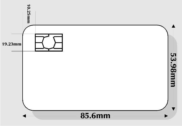
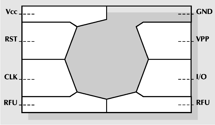
Even the name Smart Card captures the imagination, however such a term is ambiguous and is used in many different ways. ISO uses the term, Integrated Circuit Card (ICC) to encompass all those devices where an integrated circuit is contained within an ISO ID1 identification card piece of plastic. The card is 85.6mm x 53.98mm x 0.76mm and is the same as the ubiquitous bank card with its magnetic stripe that is used as the payment instrument for numerous financial schemes. Integrated Circuit Cards come in two forms, contact and contactless. The former is easy to identify because of its gold connector plate figure 1. Although the ISO Standard (7816-2) defined eight contacts, only 6 are actually used to communicate with the outside world. The Contactless card may contain its own battery, particularly in the case of a "Super Smart Card" which has an integrated keyboard and LCD display. In general however the operating power is supplied to the contactless card electronics by an inductive loop using low frequency electronic magnetic radiation. The communications signal may be transmitted in a similar way or can use capacitive coupling or even an optical connection. The Contact Card is the most commonly seen ICC to date largely because of its use in France and now other parts of Europe as a telephone prepayment card. Most contact cards contain a simple integrated circuit although various experiments have taken place using two chips. The chip itself varies considerably between different manufacturers and for a whole gambit of applications. Let us consider first the purpose for the 6 contacts used by the ICC figure 2. Vcc is the supply voltage that drives the chips and is generally 5 volts. It should be noted however that in the future we are likely to see a move towards 3 volts taking advantage of advanced semiconductor technology and allowing much lower current levels to be consumed by the integrated circuit. Vss is the substrate or ground reference voltage against which the Vcc potential is measured. Reset is the signal line that is used to initiate the state of the integrated circuit after power on. This is in itself an integral and complex process that we shall describe later in more detail. The clock signal is used to drive the logic of the IC and is also used as the reference for the serial communications link. There are two commonly used clock speeds, 3.5795 MHz and 4.9152 MHz. The lower speed is most commonly used to date in Europe but this may change in the future. One may be tempted to ask why these strange frequencies were chosen, why not just a straight 5 MHZ. The reason lies in the availability of cheap crystals used in the television world. For example the American NTSC colour subcarrier frequency is exactly 3.579545 MHz. The Vpp connector is used for the high voltage signal that is necessary to program the EPROM memory. Last, but by no means least is the serial input/output (SIO) connector. This is the signal line by which the chip receives commands and interchanges data with the outside world. This is also a fairly complex operation and will be the subject of a more detailed discussion where symbols such as T0 and T1 will be fully explained. So what does the chip contain. Well, the primary use of the IC card is for the portable storage and retrieval of data. Hence the fundamental component of the IC is a memory module. The following list represents the more commonly used memory types:
In order of increasing real estate the PROM comes next. This memory is programmable by the user through the use of fusible links. However, high voltage and currents are required for the programming cycle and such devices are not normally used in Integrated Circuit Cards. The EPROM has been widely used in the past but the name for this application is something of a misnomer. Whilst the memory is erasable by means of ultra violet light, the necessary quartz window is never available in the ICC and the memory is really used in one time programmable mode (OTP). Getting pretty heavy in real estate terms is the EEPROM. This memory is indeed erasable by the user and can be rewritten many times (between 10,000 and 1,000,000 in a typical implementation). All of these memories described so far are non volatile. In other words when the power is removed they still retain their contents. The random access memory (RAM) is a different kettle of fish, this is volatile memory and as soon as the power is removed the data content is lost. In order to pursue our studies further we must note that the cost of the IC at saturation (i.e when development costs have been recouped) is proportional to the square area of silicon used (assuming constant yield). The ISO connector is so designed to constrain the silicon die size to about 25mm2 (although it is possible to handle 35mm2 or more). The important point is more concerned with reliability since clearly the larger die will be more prone to mechanical fracture. There is another bi-product that we will consider later where the cost of testing and personalisation are considerably altered by the complexity of the particular chip. It is clear however that we should attempt to minimise the contents of the chip on both cost and reliability grounds commensurate with the particular application. Well of course you cannot have something for nothing and although a telephone card may operate with a little EEPROM memory (128 - 512 bytes) and the memory control logic, more sophisticated applications will demand ROM, EEPROM, RAM and a CPU (Central Processing Unit) to achieve the necessary business. It is the addition of the CPU or micro-controller that really leads to the term "Smart" although we will not be rigorous in our use of the term. The control logic should not be overlooked as this is necessary not only for communication protocols but also to offer some protection of the memory against fraudulent use. The ICC is probably the security man's dream because unlike most electronic storage and processing devices it has security intrinsically built in. The ICC really does provide a tamper resistant domain that is difficult to match with the somewhat larger security boxes that handle cryptographic processes. So now we can differentiate the different types of ICC by their content,
In the Smart Card world the term, application, is widely used to describe the software or programs that the IC implements. In the simplest case the application may be just a file manager for organising the storage and retrieval of data. Such an application may be totally implemented in the logic of the chip. Similarly the chip must contain the communications logic by which it accepts commands from the card acceptance device (CAD) and through which it receives and transmits the application data. The ICC which contains a CPU can handle more sophisticated applications and even multi applications since the CPU is also capable of processing the data and taking decisions upon the various actions that may be invoked. The subject of multi-applications and particularly the implementation of security segregation is another subject for more detailed discussion in subsequent parts. How the IC card is made The manufacture of a Smart Card involves a large number of processes of which the embedding of the chip into the plastic card is key in achieving an overall quality product. This latter process is usually referred to as card fabrication. The whole operation starts with the application requirements specification. From the requirements individual specifications can be prepared for the chip, card, mask ROM software and the application software. The ROM software is provided to the semiconductor supplier who manufactures the chips. The card fabricator embeds the chip in the plastic card. It is also quite normal for the fabricator to load the application software and personalisation data. Security is a fundamental aspect in the manufacture of a Smart Card and is intrinsic to the total process. We will look at each of the stages in the manufacture of the Smart Card as shown in figure 3. Chip specification There are a number of factors to be decided in the specification of the integrated circuit for the Smart Card. For the purpose of this discussion we will consider a CPU based card although the manufacture of a memory card is substantially a subset of that described here. The key parameters for the chip specification are as follows,
Card specification The specification of a card involves parameters that are common to many existing applications using the ISO ID-1 card. The following list defines the main parameters that should be defined,
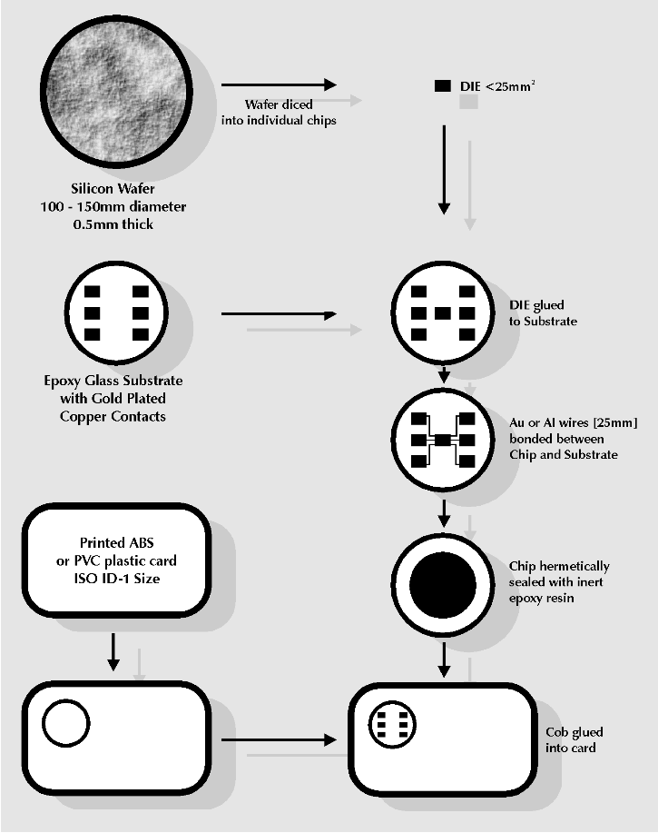
The choice of card material effects the environmental properties of the finished product. PVC was traditionally used in the manufacture of cards and enabled a higher printing resolution. Such cards are laminated as three layers with transparent overlays on the front and back. More recently ABS has been used which allows the card to be produced by an injection moulding process. It is even proposed that the chip micromodule could be inserted in one step as part of the moulding process. Temperature stability is clearly important for some applications and ETSI is particulary concerned here, such that its higher temperature requirement will need the use of polycarbonate materials. Mask ROM Specification The mask ROM contains the operating system of the Smart Card. It is largely concerned with the management of data files but it may optionally involve additional features such as cryptographic algorithms (e.g DES). In some ways this is still a relatively immature part of the Smart Card standards since the early applications used the Smart Card largely as a data store with some simple security features such as PIN checking. The relevant part of the ISO standard is 7816-4 (commands). There is a school of thought which envisages substantial changes in this area to account for the needs of multi-application cards where it is essential to provide the necessary security segregation. The developed code is given to the supplier who incorporates this data as part of the chip manufacturing process. Application software specification This part of the card development process is clearly specific to the particular application. The application code could be designed as part of the mask ROM code but the more modern approach is to design the application software to operate from the PROM non volatile memory. This allows a far more flexible approach since the application can be loaded into the chip after manufacture. Moreover by the use of EEPROM it is possible to change this code in a development environment. The manufacturer of a chip with the user's ROM code takes on average three months. Application code can be loaded into the PROM memory in minutes with no further reference to the chip manufacturer. Chip fabrication The fabrication of the card involves a number of processes as shown in figure 4. The first part of the process is to manufacture a substrate which contains the chip. This is often called a COB (Chip On Board) and consists of a glass epoxy connector board on which the chip is bonded to the connectors. There are three technologies available for this process, wire bonding, flip chip processing and tape automated bonding (TAB). In each case the semiconductor wafer manufactured by the semiconductor supplier is diced into individual chips. This may be done by scribing with a diamond tipped point and then pressure rolling the wafers so that it fractures along the scribe lines. More commonly the die are separated from the wafer by the use of a diamond saw. A mylar sheet is stuck to the back of the wafer so that following separation the dice remains attached to the mylar film.Wire bonding is the most commonly used technique in the manufacture of Smart Cards. Here a 25uM gold or aluminium wire is bonded to the pads on the chip using ultrasonic or thermo compression bonding. Thermo compression bonding requires the substrate to be maintained at between 1500C and 2000 C. The temperature at the bonding interface can reach 3500C. To alleviate these problems thermo sonic bonding is often used which is a combination of the two processes but which operate at lower temperatures. The die mounting and wire bonding processes involve a large number of operations and are therefore quite expensive. Because in general only 5 or 6 wires are bonded for Smart Card applications this approach is acceptable. However in the semiconductor industry generally two other techniques are used, the flip chip process and tape automated bonding. In both cases gold bumps are formed on the die. In flip chip processing the dice is placed face down on the substrate and bonding is effected by solder reflow. With tape automated bonding the dice is attached by thermocompression to copper leads supported on a flexible tape similar to a 35mm film. The finished substrate is hermetically sealed with an inert material such as epoxy resin. The complete micromodule is then glued into the card which contains the appropriately sized hole. The fabrication of a contactless card is somewhat different since it always involves a laminated card as shown in figure 5. The ICs and their interconnections as well as the aerial circuits are prepared on a flexible polyimide substrate. Application load Assuming the application is to be placed in the PROM memory of the IC then the next stage in the process is to load the code into the memory. This is accomplished by using the basic commands contained in the operating system in the mask ROM. These commands allow the reading and writing of the PROM memory. Card personalisation The card is personalised to the particular user by loading data into files in the PROM memory in the same way that the application code is loaded into memory. At this stage the security keys will probably be loaded into the PROM memory but as mentioned previously we will explore this in more detail later. Application activation The final operation in the manufacturing process is to enable the application for operation. This will involve the setting of flags in the PROM memory that will inhibit any further changes to be made to the PROM memory except under direct control of the application. Again this is an integral part of the overall security process. This article is continued on page
2
Links
Corporate
Home Page : Online News Home
Page
Contact Us : Other Resources : Site Listing : What's New
© 1998 Smart Card News Ltd., Brighton, England. |
