
| Smart Card
Technology: Introduction To Smart Cards
by Dr. David B Everett.
Return to page 3
The block frame The frame consists of three fields:
The prologue field consists of three bytes:
The PCB byte allows the identification of three types of block frame,
The LEN byte indicates the number of bytes (if any) in the information field of the frame. Its allowed range of values are from 00 - FE hex. This allows a maximum information field of 254 bytes. The information field is used to convey the application commands and data. The epilogue field contains the block error detection code which may be either an LRC (longitudinal redundancy check) or a CRC (cyclic redundancy check). The LRC is 1 byte while the CRC occupies 2 bytes. This option is defined by the specific interface characters. Specific interface characters. We have previously discussed the specific interface characters given by the answer to reset (ATR). The T = 1 protocol uses three of these characters to establish the necessary options before communication can take place. These bytes are assigned as follows (where i > 2),
(bit 4 - 1) = CWI (default = 13) (bit 8 - 5) = BWI (default = 4) (bit 1 = 1) = CRC option (bit 1 = 0) = LRC option (default) Waiting times The T = 1 protocol uses two waiting time parameters to help flow control,
The character waiting time may be used to detect an error in the length of a block while the block waiting time may be used to detect an unresponsive card. There is also a block guard time (BGT) which is defined as the minimum time between the leading edge of the last character of one block and the leading edge of the first character in the new block to be sent in the alternative direction. The CWT and BWT are calculated from the values of CWI and BWI coded as shown previously in the specific interface bytes by means of the following equations:
Protocol control byte The protocol control byte identifies the different types of block and carries some control information including a single bit sequence number (N) and a block chaining bit (M). Other bits are used to identify transmission errors. The PCB is coded as follows: Type PCB (bits 8-1) Function The I blocks can occur as independent blocks or as part of a chain. The "More" bit is set to indicate that further blocks are to follow. The sequence number of the sender alternates between '0' and '1' starting with '0'. The R blocks are used to acknowledge the successful or otherwise receipt of transmitted blocks. The sequence number N carries the value of the next expected value of N where the transmitter alternates the value as mentioned above. While blocks transmitted as part of a chain must be acknowledged by an R block the receipt of a successful stand alone I block may be acknowledged by an I block response. The two correspondents manage the sequence numbers of their I blocks independently alternating between '0' and '1'. The R block has three possible states as shown in the table.
The S blocks are used to invoke four control states as shown in the table. The resynch request is used by the IFD (only) to force a reset of the block transmission parameters to their initial values. A chain may be aborted by either the IFD or ICC perhaps due to some physical error such as memory corruption. The ICC may send an IFS request to invoke a change in the IFSC it can support. Similarly the IFD may send an IFS request to indicate a new IFSD it can support. The S block control also allows the ICC to request an extension to the block waiting time (BWT) that may be necessary to execute a command received in an I block. The INF field in this block contains a single byte integer value which is to be calculated as a multiple of the BWT value. In all cases the receiver of an S block should send the appropriate response block. The T = 1 Protocol in operation Using the notation of the ISO 7816 standard we can show the basic operation of the protocol. A more complete definition can be obtained from the standard.
N = Sequence number (alternately`0' and `1' ) M = More data bit
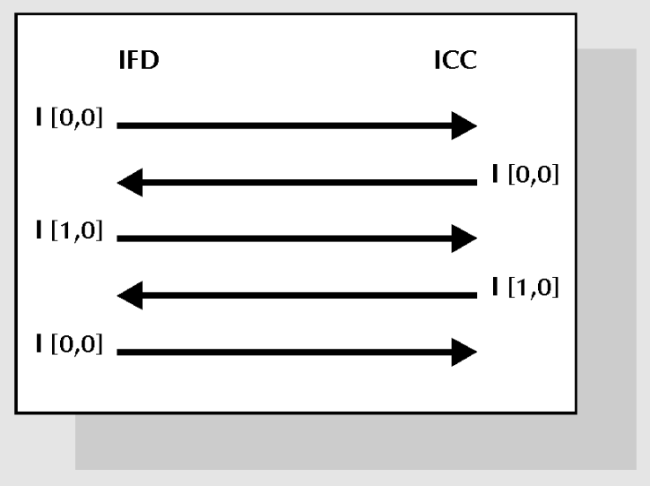
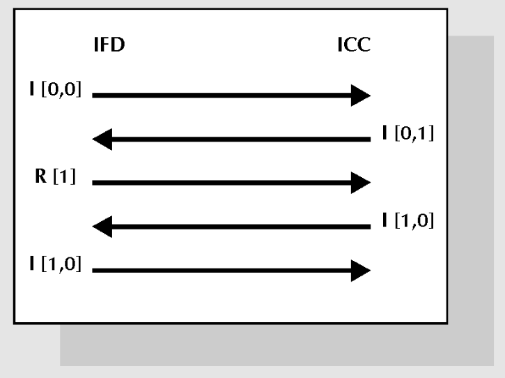
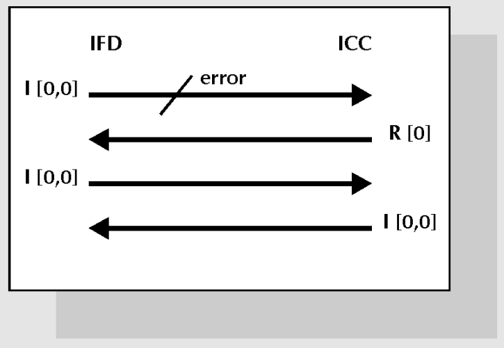
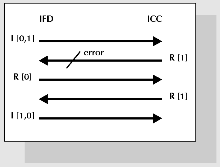
Where N = Sequence number of next expected block Normal I block transmission I Block Transmission with chaining Note that an I block was used by the ICC to acknowledge the last block in the chain sent by the IFD. The ICC may send chained blocks in the same way as shown for the IFD. Error handling in I block transmission Error in I block receipt Error in I block chain response In both cases the transmitter is notified to retransmit the block received in error. There are of course a large number of possible error scenarios but they are all based on the simple concepts shown above. Summary In this article we have given a brief overview of the technology of Smart cards. We have looked at the basic components that make up the Smart Card and have explored the elements of the chip which are at the centre of this technology. Many poeple have questioned why the introduction of Smart cards have been so slow for which the typical response has always related to the lack of standards. We have tried to show here that the standards do exist and that the central core necessary to build cards and devices are fairly well defined. It is particularly appropriate at this time to comment that there are several major commercial projects using Smart Cards such as "Mondex" (Global Electronic Cash) that are based on these ISO standards. Similarly we can now also report on the major payment schemes of Visa, Mastercard and Europay who have worked together to produce specifications based on the ISO standards for the introduction of chip cards in their varioius systems. It has been said many times before
but now at last we really are seeing the day of the Smart Card.
Links
Corporate
Home Page : Online News Home
Page
Contact Us : Other Resources : Site Listing : What's New
© 1998 Smart Card News Ltd., Brighton, England. |
|||||||||||||||||||||||||||||||||||||||||||||||||||||||||||||||||||||||||||||||||||||||||||||||||||||||||||||||||||||||||||||||||||||||||||||||||||||||||||
